

 Major customers


chemical etching process
| Introduction: | |
| Application: |


- Hotline: 86-755-61501695
- E-mail: YW1@zldsmt.com
- Contact: Selina
- Skype: julid2012
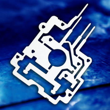
Product details
Technical Data:
Machining Type Photo chemical etching, Laser cutting, stamping and E-forming
1.Material Capabilities Stainless Steel, Brass, Bronze, Copper, Hardened Metals, Precious Metals and Aluminum alloy.
2.Product thickness: 0.001´´ up to 0.045´´3.Product Max Dimension: 27*27 inch
4.Smallest opening hole D= 0.0039 inch when thickness below 0.002´´
5.Centre to Centre for holes 1.5*Thickness
6.Chemical etching Smallest line width 0.03mm.
7.Product dimensional tolerance ± 0.01mm (depending on the thickness). It’s generally 20% of material thickness.
8.Secondary processing:Silver/Gold/Tin plated, Matt finish, paint, polishing or other surfaces treatment can be discussed when needed.
9.Two types of image files (DXF/DWG) enabled
Applications:
|
|
Benefits of chemical etching compared with stamping:
Julid completes the entire chemical etching process in-house, reducing costs and optimizing turnaround time.
Creating a phototool is significantly less expensive than creating “hard” tools like stamping or punching dies. Phototools also do not experience the wear common to hard tools, so there’s no added cost of replacing worn or damaged ones. Additionally, chemical etching allows you to bypass the secondary operations of de-burring and annealing sometimes required by stamping or drilling.
Others including:
* No need for expensive Die´s
*Can be fabricated very thin metals, thickness from .001´´ up to 0.045´´
* Pore complex and groove can also easily adjust the depth of groove
* No alteration process, the characteristics can be obtained as the designer intended
Related Products


