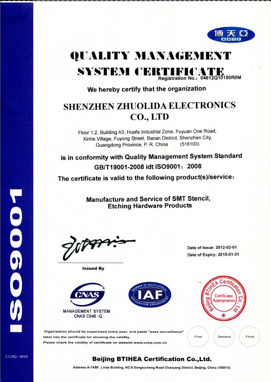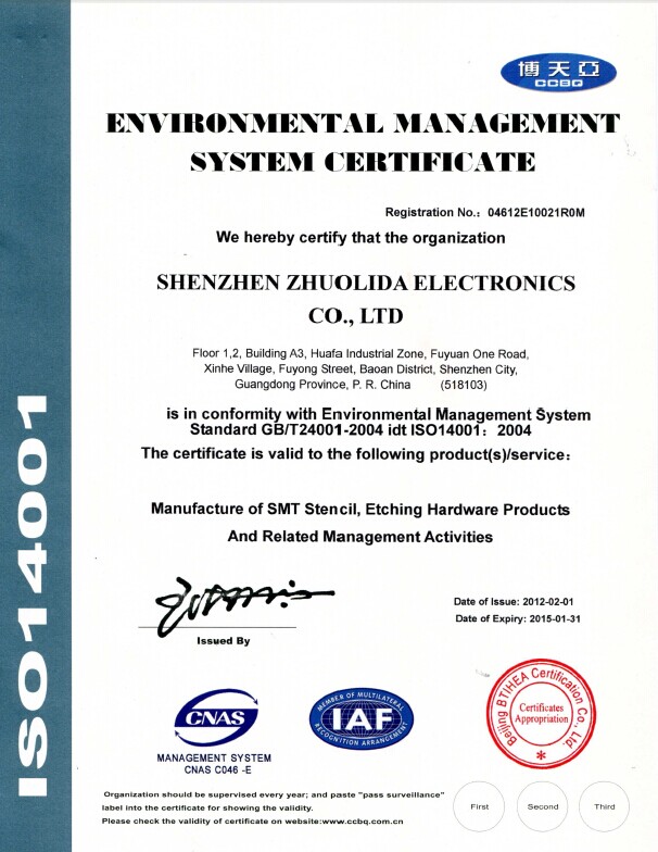
- Scan to download[More]

chemical etching company in China
Researchers in China have transferred nitride semiconductor light-emitting diodes (LEDs) grown on silicon (Si) to copper submounts, giving a 122% increase in light output at 350mA injection current [Tufu Chen et al, Appl. Phys. Lett., vol100, p241112, 2012]. The research was carried out at Sun Yat-sen University’s State Key Laboratory of Optoelectronic Materials and Technologies.
Growth of nitride semiconductors on silicon is expected to lower costs due to access to larger-diameter wafer substrates, particular for power and high-frequency transistors. For LEDs, light absorption in the narrower-bandgap substrate material needs to be avoided, for example by interposing mirror layers.
Another technique is substrate removal, which can be achieved by transfer to a copper submount and thinning/etch. Copper is attractive for this application due to its good electrical and thermal conductivity.
Such techniques were proposed by Nagoya University in Japan in 2005, giving 49% more light than before substrate removal. In 2010, Hong Kong University of Science and Technology reported a 70% enhancement from the transfer of nitride LEDs to copper.
The Sun Yat-sen University researchers began by growing crack-free indium gallium nitride (InGaN) multi-quantum-well (MQW) layers on Si (111) substrates using metal-organic chemical vapor deposition (MOCVD).
A thin interlayer of GaN was grown at low pressure (70mbar) between high-temperature aluminum nitride (AlN) buffer and normal pressure (300mbar) GaN. The aim of the interlayer was to speed the transition between the 3D growth of the buffer and the 2D (‘island’) growth favored for thin high-quality layer LED structures. Low-temperature AlN interlayers were used to control stress in the preliminary epitaxial layers.
The further epitaxial structure consisted of 0.8μm undoped GaN, 0.75μm n-GaN (1050°C), 10-periods of 2nm-thick In0.12Ga0.88N MQWs with 17nm-thick GaN barriers (880°C), and ending with a 0.15μm p-GaN cap (1050°C).
Next:Aluminium Surface TreatmentPrevious:PCMI: Photo Chemical Etching Machining Institute
Information
- 2013-03-19What is scratches? What lead to it? how to avoid it?
- 2012-11-18how to avoid the burr on metal stamping?
- 2012-11-07Do you know what is perforated signage?
- 2012-11-01etching/ chemical etching
- 2012-10-30who is the best precision etching in china
- 2012-10-26Absolute and incremental encoders
- 2012-10-25Corona Current Control by Charge Corona Grid
- 2012-10-15Semiconductor etching both performed and monitored with new U. of I. process
- 2012-09-18stainless steel etching
- 2012-09-16Stainless steel price fall sparks buyers´ defaults in Europe


